Up to the present time our studies were limited to studying the steady state circuit, calculating voltages
and currents, but without variation on the frequency of the source of the sinusoidal signal that fed the circuit.
From this moment, we are interested in studying these circuits when they are submitted to a sinusoidal voltage
source or current with variable frequency. Thus,
the idea is to keep the signal amplitude of the sinusoidal source constant at the input of the circuit,
and we vary the frequency of the signal, we analyze the resulting signal at the output of the signal.
With this, we get the so called frequency response of the circuit. Thus, we will obtain a description of the
behavior in sinusoidal steady state of a circuit as a function of the frequency.
There are two important properties that we should look at: one is like the gain function
of the circuit behaves as we change the frequency at the input of the circuit; another is the variation in
phase of the output signal in relation to the input signal.
We can express mathematically or graphically the gain and phase functions of the circuit.
It is not interesting to work with the gain function in a linear way.
Thus, it was chosen to express the gain by a logarithmic function.
A unit of measure called Bel was defined. However, since a Bel is a
very large unit, it was decided to partition it and call it the decibel .The decibel is defined
as the tenth part of Bel. So we can express the gain or loss
of a circuit in decibels.
In circuit analysis we have three related quantities that can be expressed in
decibels, that is, the power, voltage and current. The equation that defines the
gain or loss of power differs from the equation that defines voltage or current gain or loss. Then for the
power we have the equation given below.
eq. 57-01
Understand Po as output power and Pi as input power.
And for the case of voltage and current, the equations are:
eq. 57-02
eq. 57-03
This difference in the equations is due to the power being a quadratic function,
P = R I2 or also P = V2/R. Then, in the first equation, substituting
P for any of the above equations, when applying the properties of logarithms the quadratic term multiplies the factor 10 by 2,
resulting in 20 times the logarithm of the ratio between voltages or currents.
Because dB is an extremely versatile unit, many patterns have been created
referenced to different values. Let's look at four of them.
The dBm is a value created as a reference for comparing values in decibels for different systems. In communication, dBm is widely used, which establishes the value of
zero dBm when a load of 600 ohms dissipates a power of 1 mW.
In this way, on the load we will have a voltage of 0.775 volts or 775 mV.
For example, if we measure a power of 100 mW at a load of 600 ohms at the output of a circuit, the value in dBm will be:
dBm = 10 log (100 / 1) = 20 dBm
There is also dBu, which has become a standard professional audio unit. The power standard, in this case dBm, has been replaced by dBu which takes the voltage
of 0.775 V or 775 mV, no matter the value of the load.
For the same reason the dBV was created, where the reference is the voltage of 1 volt on a load of 600 ohms. These parameters set the zero dBV pattern.
For example, if we measure a voltage of 100 mV at a load of 600 ohms at the output
of a circuit, the value in dBV will be:
When we work in the field of acoustics is very used the term db SPL. SPL is the abbreviation for "Sound Pressure Level". Here the
reference is the lowest sound intensity that the human ear can perceive. This value, symbolized
per Io, has a reference level of 10-12 W/m2. Thus, the equation that allows to calculate the value in dB SPL is given by:
eq. 57-04
Then when we have a sound signal with an intensity of I = 10-12 W/m2
we say we have zero dB SPL. If I = 10-6 W/m2, then:
we call of Diagram or Bode Graphic the graphical representation of the frequency response and phase
of a system, using the transfer function representing the system response when there is variation in the signal frequency.
We must introduce some terms used in this technique that we must understand them perfectly.
One of them is the call OCTAVE.
Be a frequency signal f. If we duplicate this frequency, we say that the sign "went up" by one octave. On the other
hand, if we divide the frequency by a factor 2, then we say that the signal
"went down" by an octave. So if we say that the frequency of the signal has increased by
2 octaves, we mean that the frequency of the original signal has been multiplied by a factor
4. If 3 octaves was raised, the original signal was multiplied by a factor 8. We easily perceive that the
multiplying factor obeys the law 2n, where n is the number of octaves that has changed the
frequency of the signal. Note that when the frequency decreases,
n takes negative values.
Another term: DECADE.
Decade, as its name implies, is a frequency that is ten times higher than the other frequency taken as a reference.
Be the frequency of 1000 Hz. A decade above we have the frequency of
10 000 Hz. And a decade below we have the frequency of 100 Hz.
Another term we must introduce is: CUTOFF FREQUENCY.
Cutoff frequency is understood as the frequency at which the circuit begins to show a drop in its gain, following an asymptotic curve.
One more term: PHASE of the signal.
It has already been studied that the value of both the capacitive reactance and the
inductive reactance are depends of the
frequency of the signal to which they are subjected. The impedance of a circuit containing reactive elements can be
expressed by Z = R ± jX. And the signal phase value is given by
φ = arctg (±X/R).
Thus, it is evident that if we change the frequency of the signal we are changing the value of the reactance,
and as a consequence, we change the phase φ of the signal at the output of the circuit.
Circuits that have a gain or reduction in gain of the order of 6dB / octave or
20 dB / decade (these values are equivalent), are said 1st order circuits. Second order
circuits have values of 12 dB / octave or 40 dB / decade. If we raise an order we must add
6 dB / octave or 20 dB / decade to the previous value.
Figure 57-01
Let's look at the circuit shown in the Figure 57-01, calculating the output voltage Vo to different frequencies of the voltage source. That is, we will analyze the gain of the circuit as a function of frequency. To calculate the output voltage we will make a voltage divider. Note that the resistance in series with the capacitor forms an impedance whose absolute value can be given by
|Z| = √ (R2 + X2) and Xc = 1 / (ω. C).
Considering the frequency of 10 Hz we have |Z| = 9 947.67 Ω and
Xc = 9 947.19 Ω. Making the voltage divider, we have:
Vo = V (Xc / |Z|) = 10 (9 947.19 / 9 947.67) = 10 V
Note that for each frequency we consider there will be a new value for Z and Xc.
This will generate a new value for Vo. For simplicity we present the results in the Table 57-01 for four decades,
that is, we vary the frequency from the value of 10 Hz to the value of 100 000 Hz. With this, we can analyze how the
circuit behaves when we vary the frequency of the voltage source.
Table 57-01
Frequency (Hz)
Reactance (Ω)
Output Voltage (V)
Value in dB
Phase in Degrees
10
9 947.19
10.0
0
- 0.58
50
1 989.44
9.99
- 0.01
- 2.88
100
994.72
9.95
- 0.04
- 5.74
500
198.94
8.93
- 0.98
- 26.69
1 000
99.47
7.07
- 3.00
- 45.15
2 000
49.74
4.45
- 7.03
- 63.56
5 000
19.89
1.95
- 14.20
- 78.75
10 000
9.95
0.99
- 20
- 84.32
20 000
4.97
0.50
- 26
- 87.15
50 000
1.99
0.20
- 34
- 88.86
100 000
0.99
0.10
- 40
- 89.43
The Table 57-01 shows that as the voltage source frequency increases, the voltage on the capacitor decreases,
and for 100 000 Hz, the voltage decreases by a factor of 100 times in relation to the maximum value.
By definition, the signal decays 3 dB at the cutoff frequency of the circuit. Looking
at the table we see that this occurs at the frequency of 1000 Hz. Then, for the circuit that
we are analyzing its cutoff frequency is 1 000 Hz. On the other hand, note that
for frequencies below the cutoff frequency the output voltage is greater than 70.7% of the
maximum signal and for frequencies above the cutoff frequency the output voltage is lower
70.7%. With the data of the table we can draw a graph as shown in the Figure 57-02, with the purpose
of showing the behavior of the output of the circuit as a function of frequency. Note that in the
frequency axis we use a logarithmic scale with the unit in hertz, and the (vertical) gain axis is in dB.
Figure 57-02
From the graph we can see that in the frequency of fc/2 there is a drop in 1 dB,
and the frequency of 2 fc a drop in 6 + 1 = 7 dB. This difference of 1 dB
occurs between the theoretical curve and the actual curve.
With this example, we learned how to plot a gain as a function of frequency variation
supplied by the voltage source that powers a circuit.
Then we learn that at frequencies where the voltage gain is equal to 0.707 of its maximum value,
these frequencies are called cutoff frequencies.
Thus, in an amplifier we have a lower cutoff frequency, normally called f1,
and a higher cutoff frequency, typically called f2.
Cutoff frequencies are also known as half-power frequencies because the power at the load is
half the maximum value at these frequencies. This is because the power in the load is the quotient between the square of the voltage
and the value of the load resistance. Since the square of 0.707 is equal to 0.5, this results in half the value
of power in the midband. This characteristic is extremely important for the selection of components in audio systems,
communications and signal processing, ensuring that only the desired frequencies are amplified or
transmitted, while unwanted ones are attenuated.
Thus, midband (or passband) of an amplifier is defined as the band or range
of frequencies that is located between
10 f1 and 0.1 f2. In the midband we can say that the gain of an amplifier
is maximum, and we will call it Avm. Thus, we can state that there are three important characteristics in a
amplifier: one being the gain in the midband, or Avm and the limiting frequencies, that is,
f1 and f2.
Typically we want the amplifier to operate in the midband. However, there are situations in which you need to know how it behaves.
before or after the cutoff frequencies, i.e. outside the midband. So, knowing the values of Avm,
f1 and f2, we can calculate the amplifier gain for any frequency f.
Therefore, we can have two situations described below.
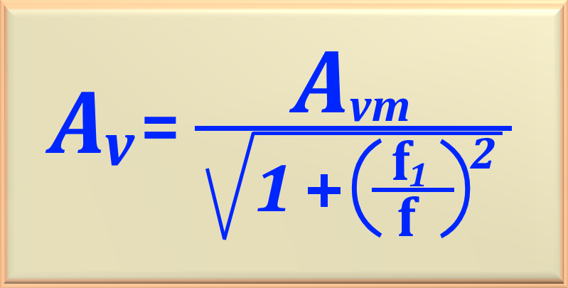
1 - Response Below Midband
Below the midband we can determine the gain Av of the amplifier through eq. 57-06.
eq. 57-06
2 - Response Above Midband
Above the midband we can determine the gain Av of the amplifier through eq. 57-07.
To complete this study, we must present a graph showing the phase variation of the output signal as a function of frequency.
In the table above, the right column represents the phase.
The phase is calculated from the voltage divider equation using the appropriate phasors.
Vo = [ V (Xc ∠ -90 ) / √ (R2 + Xc2)]
As we are interested in the phase θ, algebraically working the equation above
in the form Vo / V we arrived at:
θ = - arctg (R/Xc)
The angle θ represents the phase difference between Vo and V.
Since the value of θ is always negative, except for f = 0 Hz, the voltage
Vo is always delayed with respect to V. Hence this circuit is known as
lag circuit. In the figure below we can see the graph of the phase.
Note that in the cutoff frequency the phase of
Vo is delayed with respect to V of 45°. We know that in this frequency
XC = R, resulting in a quotient between the two variables equal to 1. Hence, we easily
conclude that θ = 45°, because arctg 1 = 45°.